Perpetual Paper
An Ultra-Low-Power E-Paper Persistent Digital Picture Frame
by Evan Shaw
Background
I’ve been interested in electronics and digital design since I took Purdue’s CS250 Computer Architecture. Combining this with my love of C programming synthesized my interest in embedded hardware and software design. During my university days, I put hundreds of hours into independently studying electronics, somewhat to the detriment of my computer science curriculum. But all this study was no good without a large project to show for it. In 2021 I saw this video: Trolling My Mom With an E-Paper Picture in which the creator “CNLohr” designs an E-Paper picture frame and presents it to his mother as a normal picture frame, but the image changes overnight, thus the 'troll'.
This was the perfect project for me to learn embedded development. It involved integrating multiple different chips with serial protocols, and the result would be a novel project that could actually do something. I set to work… 3 years later. In 2024, I purchased the same Waveshare 7-Color AceP E-Paper module in June, planning on completing this project in about a month; just in time for my mom’s birthday. Unfortunately I underestimated the amount of work that would be involved, and overestimated my technical abilities in this department, and did not hit the deadline, so I decided to continue the project in 2025.
Design
I didn’t want to simply copy the project exhibited in the
inspiration video, I wanted to create my own version from scratch,
even if that meant selecting alternate components. In the video,
CNLohr mentions that his device has a quiescent current of 40µA
which is not as optimal as possible. To put a novel spin on my
project, I decided to aggressively pursue a lower quiescent current
design. The device should be in sleep mode for 23 hours and 59
minutes a day, so any improvement in resting state power consumption
would be an enormous boon. 24 hours × 40µA = 0.96 mAh,
which over the course of a year would add up. CNLohr also decided to
bitbang both the SPI protocol for interfacing with the E-Paper
module, and the SD protocol. I decided to use the hardware
interfaces for both of these protocols to save power.
Design Requirements & Component Selection
The goal of the project was to create a battery powered E-Paper picture frame that refreshes once a day, then goes to sleep in an ultra-low-power mode to conserve battery life. Preferably, the battery life should be measured in months. The images displayed on the picture frame should be stored on a microSD card in the frame. These requirements mandate that we have the following components:
- Microcontroller
- RTC functionality (for waking up the device)
- E-Paper Display
- SD card
- Battery
Microcontroller
This was my first project in which I had to choose my own micro. In past projects, I had simply used a Raspberry Pi with its GPIO pins, or the Raspberry Pi Pico. I learned that component selection is a bigger undertaking than I previously imagined. The first microcontroller I checked out was the familiar and beloved Pi Pico. Its dual core ARM M0+ combined with its expansive IO capabilities made it more than formidable to handle the data transfer involved. Unfortunately, the lowest power sleep mode of the Pi Pico is apparently around 40µA, which would have conflicted with my goal of achieving lower quiescent power than the project in the video.
There is no master spreadsheet (that I am aware of) detailing the power consumption of the deepest sleep modes of every microcontroller in existence, and me being generally unfamiliar with the product lines of the major manufacturers made the search a bit lengthy. I finally settled on the STM32L4 line, STMicroelectronics’s line of low power 32-bit Arm Cortex M4 microcontrollers. These micros have many serial interfaces, including the SPI required for the E-Paper module. They also boast a current draw in the low hundreds of nanoamps in Standby mode with RTC functionality. At 245nA, this would make it about 160 times less quiescent current draw than CNLohr’s version.
RTC
While looking for an STM32L4 development board, I discovered the NanoSleeper, a ‘feather’ development board created by Jake Wachlin that includes an STM32L412 along with a Microcrystal RV-3028-C7 ultra-low-power RTC chip. This external RTC runs at a current of ~45nA, and using its external interrupt functionality to wake up the STM32L412 instead of using the integrated RTC allows us to instead put the microcontroller into shutdown mode, consuming just 16nA. Going from 245nA consumption with the integrated RTC to 16nA for the microcontroller in shutdown mode plus the 45nA for the external RTC results in a 61nA quiescent current, a reduction by a factor of 4.
SD Card
For the storage of the images, there was no question that interfacing with an SD card would be the best way to go. They are small, and very cheap. Each image is less than ¼ of a megabyte, so any capacity in the gigabyte range would be sufficient. The standard way to interface with an SD card is the SD/MMC protocol. Many SD cards also support SPI mode. I was originally going to use SPI mode until a design decision I made. Keep Reading to Find Out What Happens Next!!!!
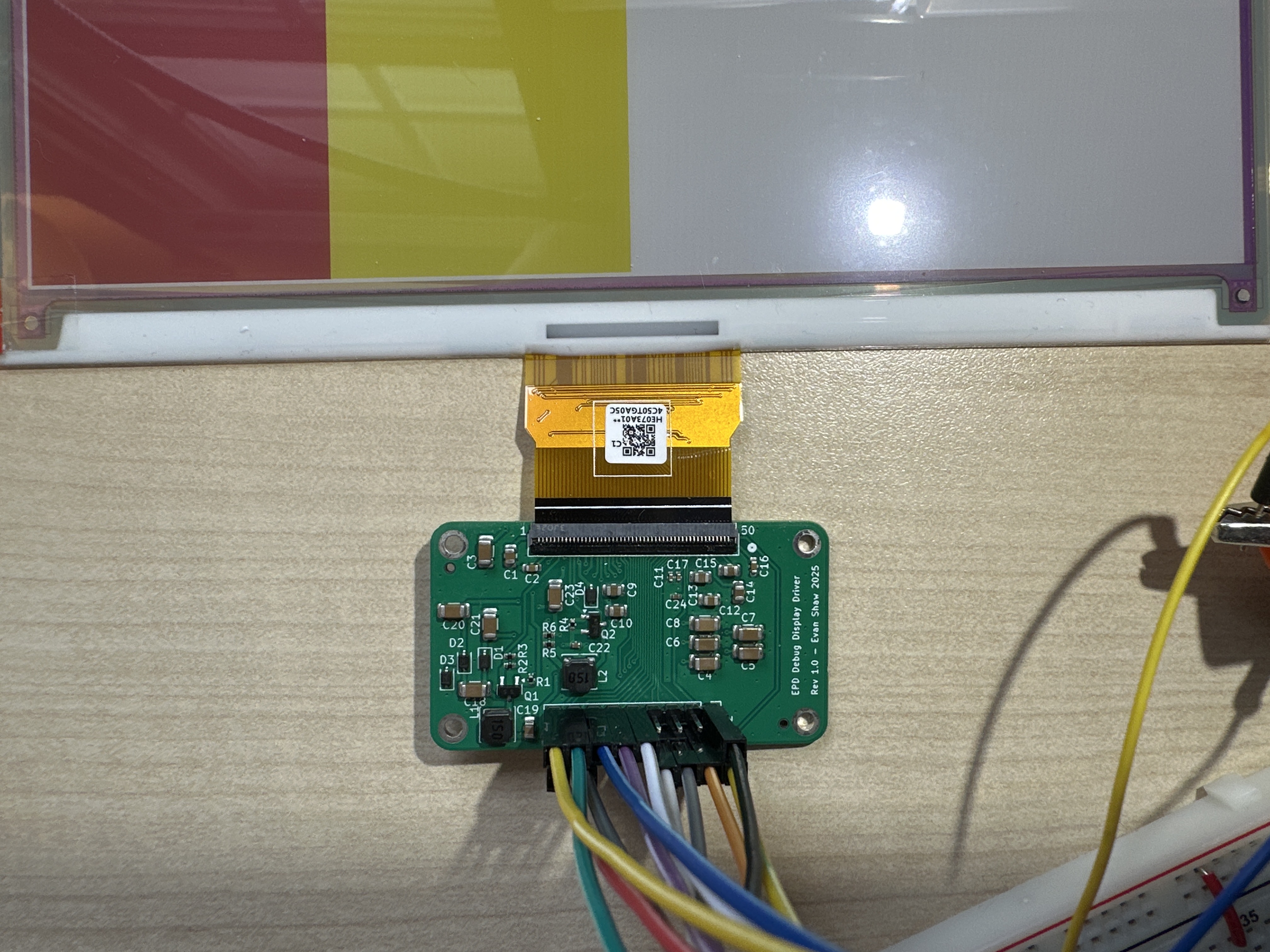
E-Paper Display
There are very few color e-paper modules available, and there are even less that are within a sane price range. The only two on the market are the E-Ink ACeP 7-Color E-Paper and the E-Ink Spectra 6 6-Color E-Paper. Both of these are manufactured by the company E-Ink, and distributed through Waveshare, an online hobby electronics retailer. Both displays are 7.3 inches diagonal, and boast a resolution of 800x480. The ACeP 7-Color display came out in 2021, while the Spectra 6 6-Color came out in 2024, dropping a color, but improving the contrast between colors. When I started this project I had already committed to using the ACeP 7-Color module, but I believe they are pin compatible, and only a minor software change would be needed to switch to the Spectra 6.
Waveshare offers the ACeP 7-Color display module (hereafter referred to as ‘the display’) for $67.99, and a version including the ‘hat’ interface board for $75.99. The hat allows easy attachment to the GPIO pins of a Raspberry Pi, or a simple data and power connection with a breakout cable to DuPont connectors.
Power
I went with a simple 2500mAh Li-Po battery from Adafruit to power the picture frame. To my understanding, there are different battery types with better self-discharge characteristics like LiFePo batteries, but there are no LiFePo batteries in small form factors, and the smallest cells I found online would require me to build a custom BMS. I’m sure I am capable of building a custom BMS, but any mistake on my part could mean catastrophic failure, and this was a bit outside the scope of the project. The 2500mAh Li-Po battery charges up to 4.2V and has internal protection circuitry that prevents discharge below 2.8V.
Issues
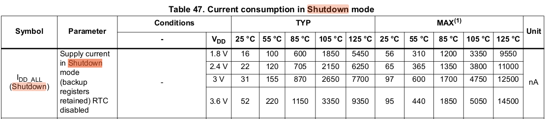
Now that I had all the individual components, I could put them together, program the frame, and call it a day, right? Well not quite, there were several areas that I wanted to improve. The first area was the voltage at which the microcontroller operates. The STM32L4 series can operate at between 1.71 V and 3.6V. I wanted the project to operate at 1.8V so the microcontroller would consume as little quiescent current as possible, and so that power consumption used by the core would be reduced during the normal run cycle. Table 47 from the data sheet shows that operating the microcontroller at 1.8V at room temperature nets between a 2-4 times reduction in quiescent current.
The only problem with doing this is that the e-paper display module apparently operates off of 3.3V power and logic. Thus a level shifting chip must be used. Another complication is that SD cards, while technically supporting 1.8V operation, must be initialized with a 3.3V power source, then sent a command to operate off of a 1.8V supply.
Upon receiving the e-paper display and the NanoSleeper feather board, I downloaded the STM32 compatible driver code from Waveshare to test the display.
I plugged everything in, modified the code a bit so it would compile, and turned on my power supply. Immediately I read a power consumption of about 1.2 Amps! I thought that this was a lot, especially if the display module wasn’t actively updating. I fiddled around with the code, and nothing seemed to fix the issue, so I powered up my oscilloscope to check that my SPI was actually sending out the correct data. What I found was a mess of crazy noise and insanity. After a few days of trying various things, I concluded that this display module I had bought the year prior, was somehow dead, despite me never using it. I ordered a new one. Once It arrived, I plugged it in, and the exact same thing happened! Either I had received two defective modules, or I was doing something wrong. I cast my mind out to potential stumbling blocks that I hadn’t thought of before, and I realized that I had plugged in the FPC connector to the display module the wrong way! When you purchase the display module with the hat board, it comes with an extra female-female PCB to connect the hat board to the display module with an extra ribbon cable, which came pre-connected to the expansion board. The FFC has contacts on only one side, and they faced up, and connected to the top of the FPC connector on both PCBs. I assumed (stupidly) that the contacts on the display module FPC should also be facing up, connected to the top of the FPC connector. This was not the case. Flipping it around made it work perfectly when displaying solid colors, and the 7-color test pattern.
At the default 4 MHz clock speed of my microcontroller, the driver took around 40 seconds to transfer the 192000 bytes. This was much longer than should have been theoretically possible, given an SPI clock division of 2 (yielding a 2 MHz clock), transferring 192000 bytes × 8 bits = 1536000 clock cycles, which should have taken less than a second. I looked into the driver code, and instead of using a sensible data transfer method, the driver used a blocking HAL function to transfer a single byte at a time. As soon as I saw this, I resolved to rewrite this code. The most optimal way to rewrite would be to have two simultaneous DMA transfers to get data out of the SD card, and to the display module. Unfortunately, the STM32L412 only has a single SPI interface, and no SDMMC interfaces, so it would be impossible to have simultaneous DMA streams.
As stated previously, the e-paper display module apparently operates off of 3.3V power and logic. Before I committed to a level shifter chip to convert the 1.8V logic from the microcontroller to the 3.3V logic used by the display module, I took a closer look at the connectivity specifications of the display module.
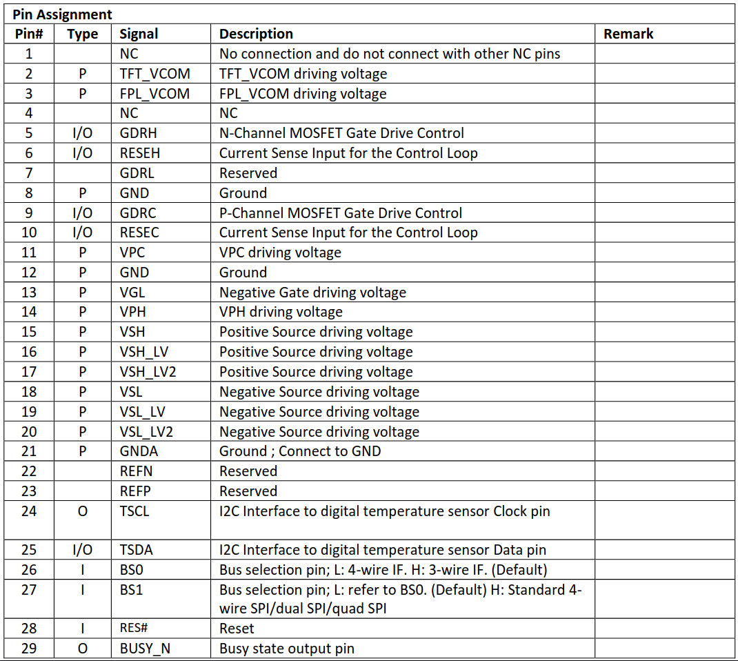
Most of the pins are connections to external capacitors and switching power supply circuits. There are a few interesting things here. First, is the potential existence of a QSPI interface, as indicated by the description on Pin 27 BS1 “Bus selection pin; L: refer to BS0. (Default) H: Standard 4-wire SPI/dual SPI/quad SPI”. There are three unused serial data pins, Pins 34, 35, and 36. The other interesting pin is Pin 40 VDDIO with a description of “Supply Voltage”. In the datasheets for other unrelated chips, VDDIO is an input pin which allows you to run the IO of the chip at a different voltage. This would solve the issue of level shifting to the device.
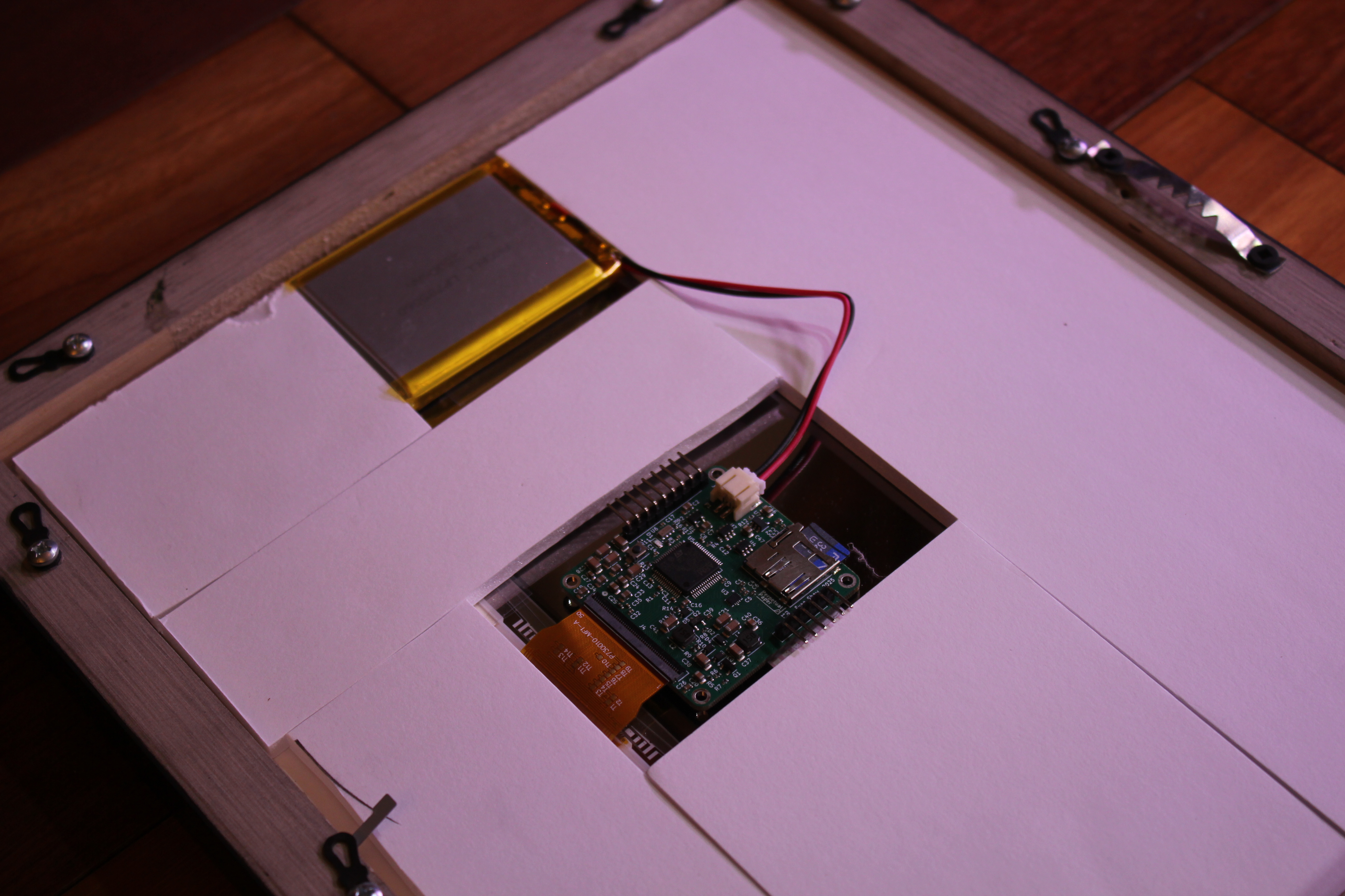
Because of the lack of two SPI interfaces conflicting with my goal of programming a simultaneous data transfer operation, I decided to upgrade the microcontroller. I couldn’t find a feather board with an upgraded microcontroller and the RV-3028-C7 RTC, so at this point, I decided to roll it all into a PCB. I had never designed a PCB, so this would be quite the learning experience. Before I designed the final PCB, I wanted to make another board to prototype the passive and active components that I would be using for the switching power of the display module.
The prototype driver board implements the circuits enumerated in the Application Note Reference and the HAT Schematic Diagram. This consists of many capacitors to hold up different voltages generated and used by the display module. There is also a boost converter to convert to higher voltages, and a buck-boost converter to convert to negative voltages. I broke out the all the relevant data and power pins, including the 3 unused data pins, the VDDIO pin, and the I2C pins of the internal temperature sensor. The board is a two-layer board, with ground fill on both sides connected with stitching vias.
I sent this design off to to JLCPCB which I chose because of their integrated PCB manufacturing and assembly services. They apparently have some arrangement/connection with LCSC, and if you use parts form LCSC, there is virtually no wait to start the assembly phase. I got my board less than a week after tapeout, and successfully powered the display module.
I tested if inputting 1.8V into VDDIO allows the SPI interface to operate at 1.8V, and this appeared to be the case! I also attempted to get the alleged QSPI functionality working by sending the same commands byte by byte, with the hardware QSPI interface, but it was not successful. The prototype display driver told me that this arrangement of the power components for the display would work, and also confirmed that the VDDIO worked like I thought it did, so I could bypass using one level shifter chip. It was time to move on to the final board design.
Final Board Design

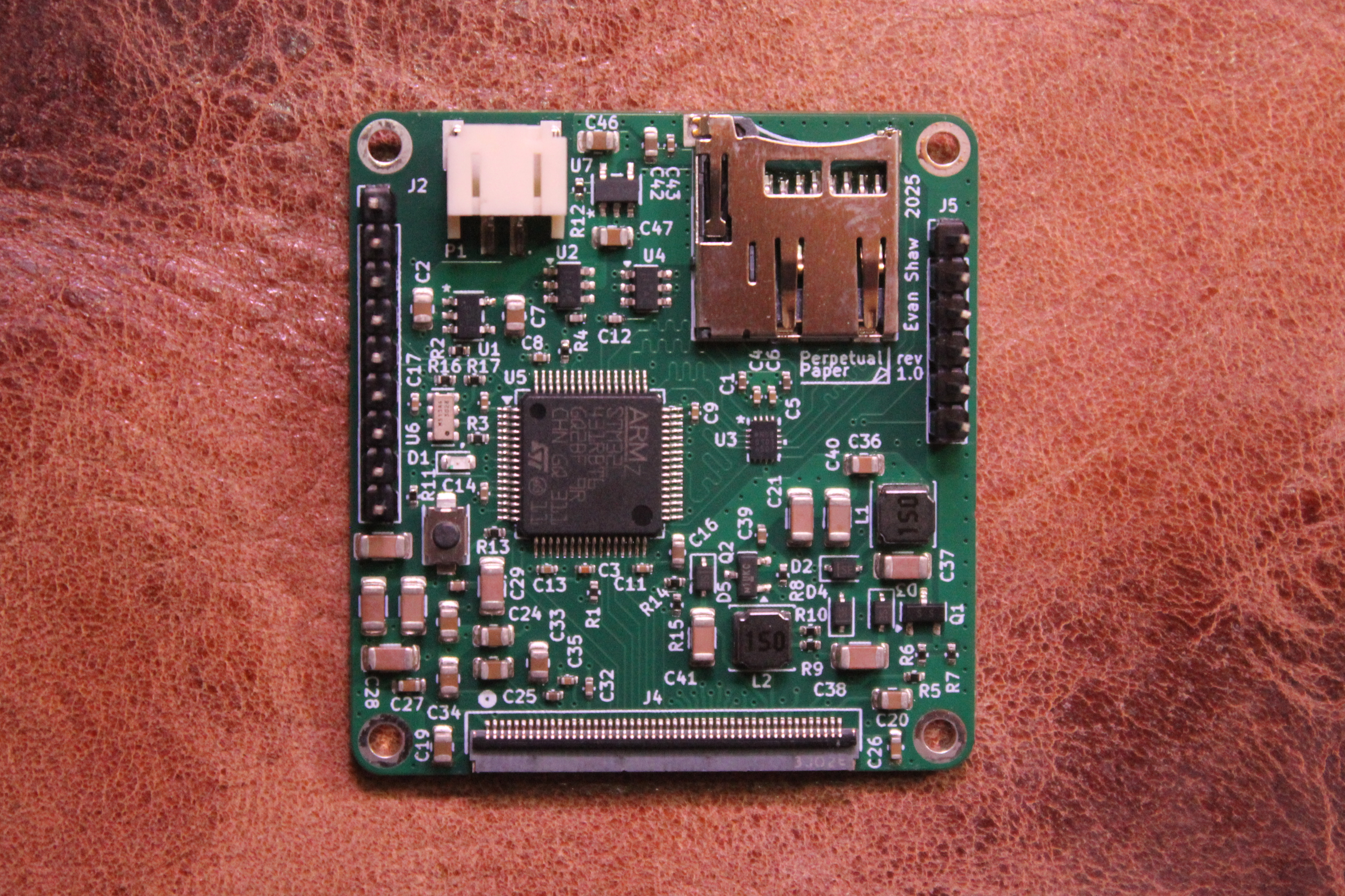
For the final PCB design, I switched to the STM32L431RB. This model adds an SDMMC interface over the STM32L412. All microSD cards must implement the SDMMC interface, while some manufacturers do not implement the SPI interface, so going with an SDMMC interface is more reliable. The 431 has 128Kbytes of flash and 64Kbytes of SRAM.
The STM32L431RB runs off of 1.8V power, which is produced by a TPS7A02 LDO connected directly to the battery. Since the microSD card needs to operate at 3.3V, I have added an NVT4858HKZ SD card voltage level translator chip to convert from 1.8V signals to 3.3V signals.
Click the preview to expand. Close with the button, Escape, or click outside.
The NVT4858 is a rather expensive chip at ~$1.00 that has high speed signal conversion capability, auto-direction control and built-in pull-up resistors and ESD protection. The amount of data transferred for each picture displayed is 192000 bytes, which is not very much, so the hight speed aspect of the chip is not entirely necessary, but I decided to add it anyway because of built-in ESD protection. I found it difficult to find reference PCB layouts for the 4-wire SDMMC interface. I couldn’t find anything put out by ST Microelectronics detailing the sufficient ESD components recommended, and decided that this chip, despite being expensive, solved a few of my problems at once.
The NVT4858 requires two voltage inputs corresponding to the voltage levels. The 1.8V level is provided by the 1.8V regulator through a TPS2291DBV load switch, and the 3.0V input level is provided through another TPS2291 load switch connected to another TPS7A02 LDO at 3.0V. I chose to add this 3.0V regulator instead of the standard 3.3V because of the range of battery voltage levels. The Li-Po battery charges up to a voltage of 4.2V, and discharges all the way down to 2.8V where internal protection circuitry cuts off further discharge. I went with 3.0V to avoid operating the regulator in dropout mode if the battery voltage was under 3.3V. The regulation provided by an LDO dramatically worsens in the dropout phase of operation, and I was worried that the supply voltage might fluctuate in this state. The capacitance on the output of the regulators and the decoupling caps at the inputs of all the chips are probably sufficient to attenuate any voltage sag that would be caused by a 3.3V regulator operating in dropout, but I decided to go with this conservative approach.
While not in use, the microSD, level shifter, and display module are all powered down by the TPS2291 load switches to reduce unnecessary power consumption. Each TPS2291 consumes around 10-100nA in off mode.
The microSD connector has an integrated switch connected to ground which is normally closed. When a card is inserted, it opens, and the 100MΩ pullup pulls the voltage high. This line is connected to a pin on the microcontroller that is configured to wake up the micro from shutdown. Therefore, inserting a microSD card is one of the five ways to wake up the device.
The microcontroller is connected to the 7.3inch 7-Color E-Paper Display Module through a master transmit-only 4-wire SPI interface. This interface is one way, data cannot be sent from the display to the microcontroller. The 4 wires involved are:
- Data Out – All data is relayed with this wire
- Clock – Clock signal that dictates timing
- CS – When the Chip Select line is low, data transmitted on the bus will be read by the display
- Data/Command – This line differentiates between a command byte, which tells the display what operation to perform, and a data byte, which is input data for the display as part of a command
There is also an I2C interface on the display module that accesses the integrated temperature sensor, which I have connected to the microcontroller.
The RV-3028-C7 RTC chip is connected to the microcontroller with an I2C bus, allowing bidirectional communication and configuration. The RTC’s INT pin is connected to a pin on the microcontroller configured to wake it up from shutdown. By setting the alarm function on the RTC, we can achieve daily wakeup to change the image.
The last two components of note are the button and the LED, both for simple user input and output.
Click the preview to expand. Close with the button, Escape, or click outside.
Before going to layout and routing, it is absolutely essential that you choose your components and make sure that you can SOURCE them. When designing the prototype driver board, I made the mistake of choosing some components that couldn’t be sourced from LCSC, and choosing arbitrary parts instead of the JLCPCB ‘Basic Parts’. I had to go back and reevaluate components I selected, which cost some time.
Layout
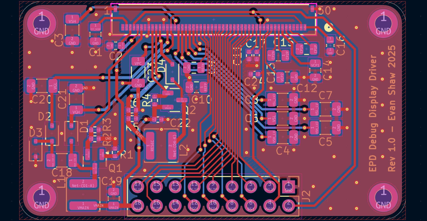
The final PCB was designed in KiCAD, just like the display driver prototype board. This time, I decided to go with a 4-layer board stackup. I could have definitely gone with two layers, but that would make routing a bit more tricky, expand the size of the board, and I had already done a 2-layer board, and wanted the experience of designing a 4-layer one. Components are only on the top layer. The top layer is a signal layer, layer 2 is the ground plane, layer 3 is the power plane (split between 1.8V, 1.8V switched, and 3.0V switched), and layer 4 is another signal layer with ground fill.
I did placement and routing entirely by hand, which was quite the challenge as I opted for the smallest design possible, not for any real reason, just to see how small I could make it. I placed down the display module connector first, then the caps and switching components for the display module. I followed that by placing the microcontroller, then the microSD connector and level shifter. You can see that I length-matched the SDMMC data lines to within 5mm of each other, which wasn’t strictly necessary for the max speed of 50MHz that this interface could possibly see, but I did it anyway for the experience. And the squiggly lines look cool.
The final parts of the board layout I did were the power components. These were very easy to route, as layer 3, the ‘power plane’ was mostly clear of other signals. Power is sourced through a 2-pin JST connector.
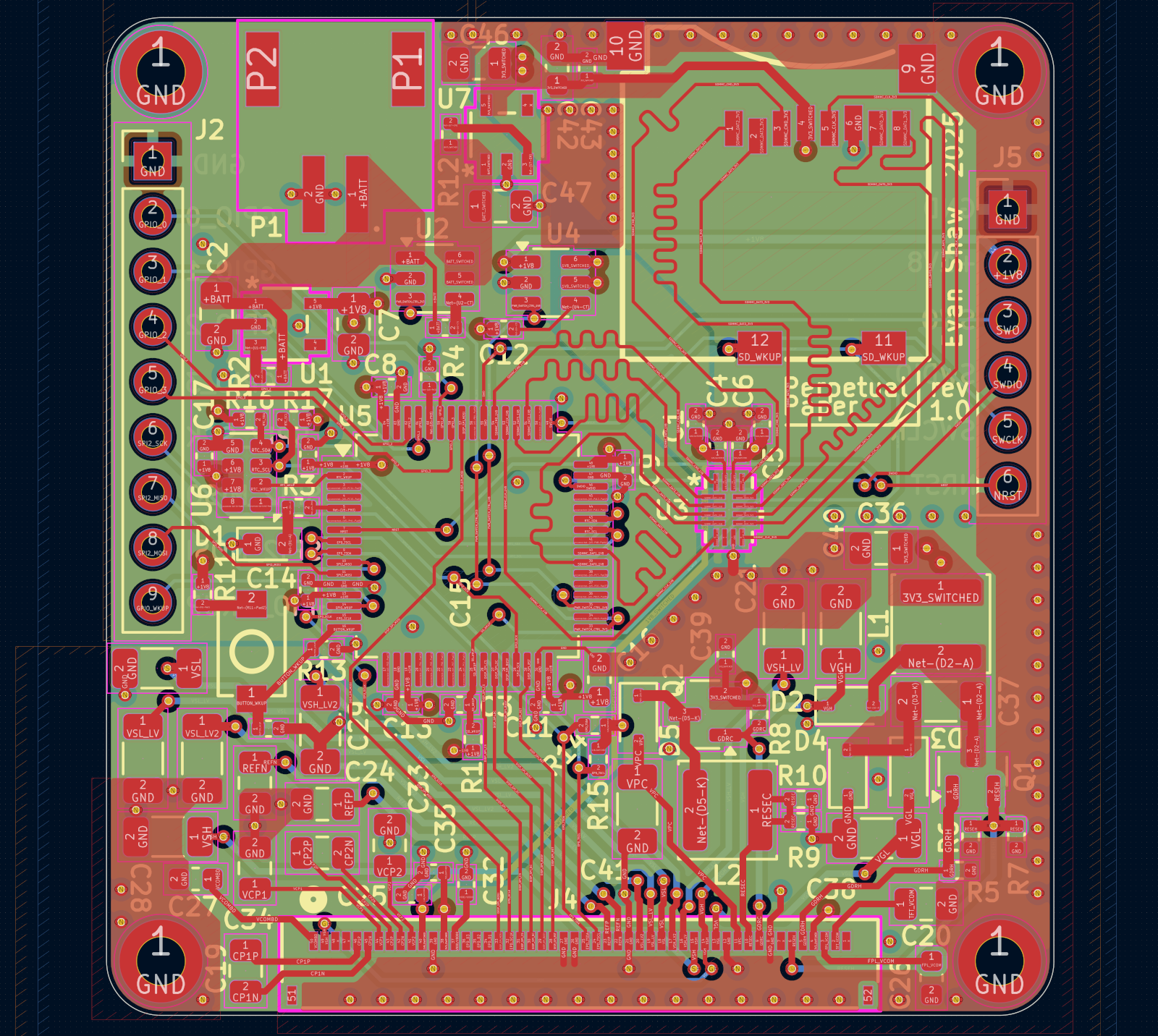
Overall, I think the layout turned out nicely. I was a little inconsistent on the ground fill on the top layer, and I just sort of put stitching vias in random places. These certainly aren't deal breakers. The board looks very good; there is hardly any unused space.
I got the boards from JLCPCB about 11 days later. I made test programs to make sure each subsystem worked.
While testing the operation of the e-paper display, I created a test pattern consisting of horizontal lines, one pixel wide, alternating colors. This test pattern would occasionally fail during the update cycle, freezing the display with incorrect colors. I debugged this issue for a few days. I checked the code, ran the driver I wrote and the manufactureres driver, probed the serial connection, and looked at the power rail voltage on my scope. I couldn’t find the issue. I concluded that since I had plugged in both of my displays backwards and ran an incredible amount of current through them, they were probably broken, and so I ordered my third display module.
I ran the same tests on the new display module, and the exact same issue happened! It took me a few hours to finally realize that my benchtop power supply has a default current limit of 100mA, and during the refresh cycle, the current usage would spike above 100mA. I’m not sure how I didn’t see the voltage sag on my scope, but setting a higher limit fixed the issue. This absolute debacle cost me about a week.
Software and Operation
When a battery is connected, the microcontroller starts running its program from flash. The program immediately checks how it was woken up. There are 5 total wakeup sources:
- Power On/NRST
- RTC: The RV-3028 is connected to the microcontroller via its INT pin. When the RTC pulls this line low, the internal pullup in the microcontroller is overriden, triggering a wakeup
- Button: A button on the board connects a pullup resistor to the microcontroller and the larger value pulldown resistor plus a de-bounce capacitor
- SD card insertion: A mechanical switch normally connected to ground, housed in the SD card connector, is opened upon card insertion, allowing the high value pullup resistor to bring the voltage high, triggering a wakeup
- GPIO pin: The pin labeled
GPIO_WKUPon the silkscreen is connected to a pin on the microcontroller that allows wakeup interrupts. It is not currently configured to do anything
Most of the wakeup sources do something slightly different. Connecting a battery shows up as a Power On/NRST wakeup. This is the base case of wakeups, which resets the RTC and sets the alarm and interrupt functionality. Waking up from an RTC sourced interrupt simply resets the alarm flag, and continues with refreshing the image. Pressing the button on the board triggers a wakeup, and a picture refresh. Upon waking up, if the program detects that the user is holding down the button, it goes into the alarm time adjustment state. Every 2 seconds, if the button is still held down, the LED blinks 3 times, and resets the alarm to trigger one hour prior.
Once the program decides that it needs to refresh the image, it
turns on both of the TPS2291 load switches, giving power to the SD
and the display module. The program mounts the FAT filesystem, and
checks for the special folder PPPhotos, and the
instruction text file inside that folder. If either of these are
missing, they are created. The instruction text file is hardwired
into the code. It then checks for the state file, a simple text file
that contains a single integer representing the name of the next
image file to be read. Then it attempts to read the file with that
name plus the file extension .ppp.
The image file is then read into memory and serialized out on the SPI interface to the display module in a double buffering scheme. The program reads data from the SD card in blocking mode (I couldn’t get DMA write to work with the SD card, only DMA read, but I think they both have to be the same mode, so I had to revert to blocking mode. This shouldn’t be that much of a performance hit) into the RX buffer. The buffers are swapped; the RX buffer becomes the TX buffer, which is transmitted via DMA to the SPI interface. A function is set to toggle a lock when the DMA SPI transmission completes. Then another block is read into the now RX buffer, and after this is done, the program busy-waits for the aforementioned lock to clear. This way, even though we are using a blocking read to get data from the SD card, the DMA SPI transmission is happening simultaneously. No processing needs to be done, as the file format is already in the correct byte arrangement the display module expects. Once the display is refreshed, the load switches are shut off, cutting power to the SD card and display module. The internal pullup is configured for the RTC INT pin, and all the appropriate wakeup sources are enabled before the microcontroller is finally shut down.
Images
Now, 7 colors is not a lot of colors. Modern displays can output tens of millions of colors. Given this example image:

If we simply convert each pixel to its nearest equivalent in our 7-color color palette, the results look something like this:

This looks simply atrocious. The main problem is the color banding, where similar colors next to each other are all converted into the same color, creating horrible looking blobs. What we need is color blending. Enter ‘dithering’, a process which blends colors together to make the perception of more colors, similar to Pointillism. The most prominent dithering algorithm is the Floyd-Steinberg algorithm. After passing through Floyd-Steinberg, we get this:
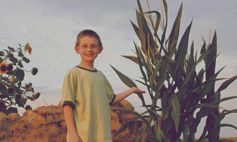
Even through the previous two images use the same color palette, the dithered image looks much better.
The pipeline to convert images like this is a bit extensive. First, we must crop and resize the image to get 800 x 480, then we must dither the image with a 7-color palette. If the dithered image looks suboptimal, we have to go back to the cropped and resized image, apply some image transformations, and dither again. Doing this for 1 picture isn’t too bad, but doing it for 365 pictures in a tool like GIMP would take all day. That is why I have programmed a photo cropping and dithering program to breeze through the crop and dither operations with a GUI.
Final Results
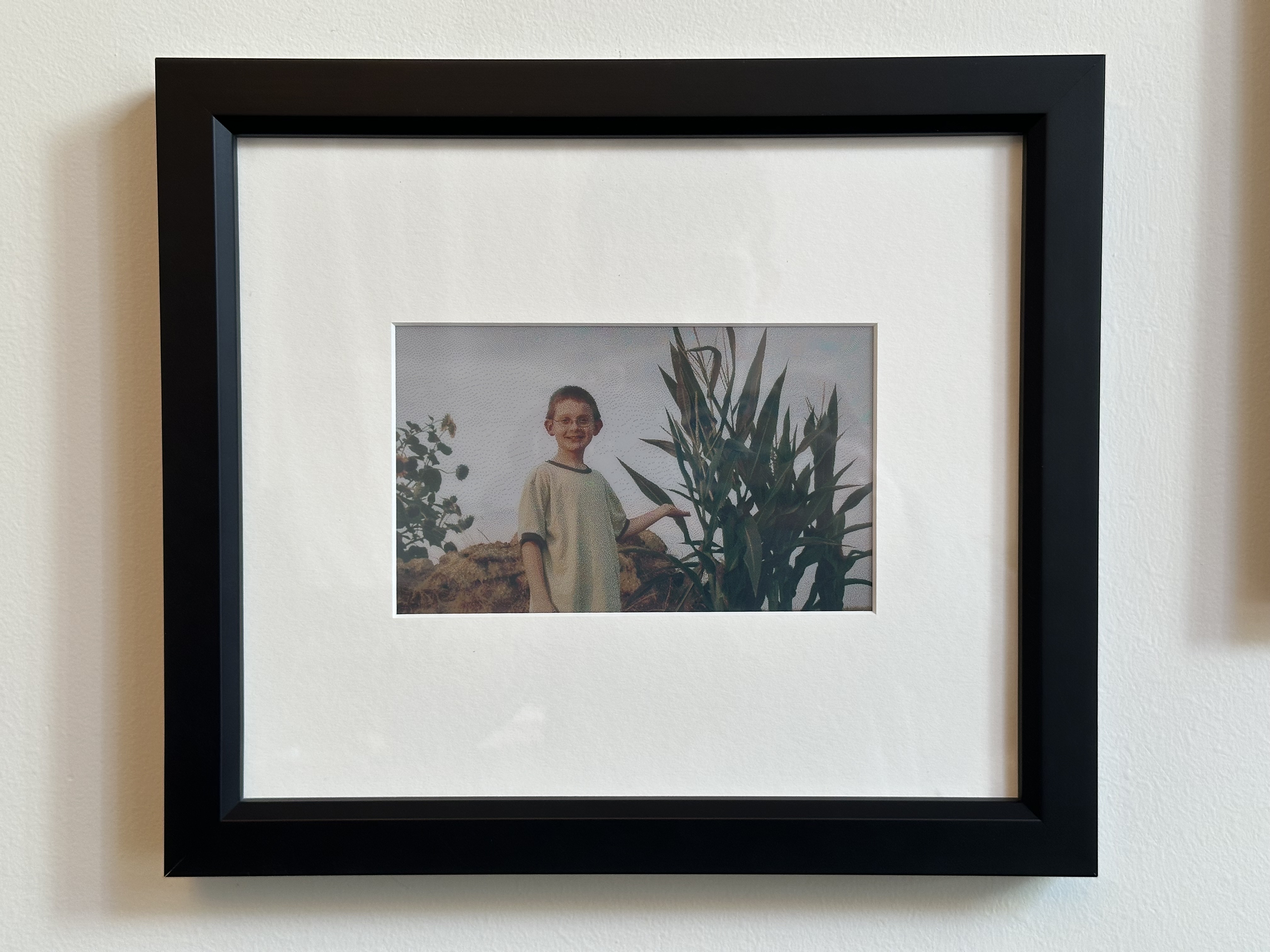
I got the final board + display + battery assembly professionally framed at a local frame shop. I went with a black frame with a white matte because I think that this color scheme is mostly picture neutral.
Power Consumption
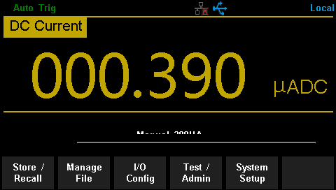
The final current consumption (quiescent current) for the Perpetual Paper in the shutdown mode at a battery voltage of 3.7V is 390 nA! This is about a 100x reduction in current from the inspiration project’s consumption of 40 µA.
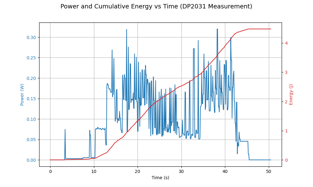
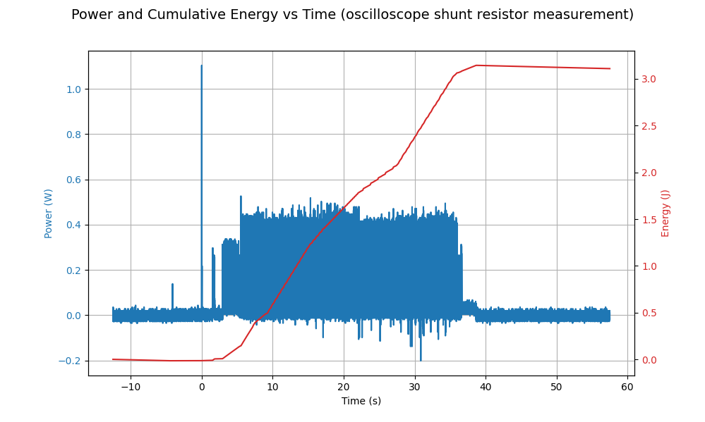
I measured that it takes between 2.5 – 4 joules to refresh the picture every day. Each individual picture takes a different amount of power, due to the arrangement and color variation of the pixels. I measured the energy used with the data from my DP 2031 benchtop linear power supply, and also by measuring the voltage drop over a shunt resistor with my oscilloscope. For the same picture, the oscilloscope appears to be reporting less power consumed than measurements from the power supply. I ran many of these tests and the example measurement here is a bit on the high side:
The 2500mAh battery at an average voltage of 3.7V yields a theoretical capacity of 33,000 J. The quiescent current of 400nA × 3.7V battery voltage × 24 hours = 35520 hnAV (hour nanoamp volts) or 0.128 J of quiescent consumption per day. With an estimate of 4 joules per refresh plus the quiescent current, 4.128 J per day gives us a theoretical battery life of 33,000 / 4.128 = 7994.18 days, or 21.9 years of operation. Of course, the battery will not last this long. If we assume self-discharge for LiPo batteries as 5% of max capacity per month and assume a constant discharge voltage of 3.7V, then I have calculated that the battery will last 1.51 years. I could do a much more extensive study to try and predict battery life, but that would involve me recording the power consumption of every photo to get a good average. However, I am waiting on an Ethernet switch to connect my power supply and scope to networking so I can easily script these operations. I would also have to do some measurements and tests on the battery, and at this point, I just need to move on with other projects. I am quite interested to learn just how long the battery lasts. My personal prediction is that it will last at least 6 months. I think this is a good enough timescale to justify not putting a charging port on the back.
I still need to make power measurements without the display connected to see how much power the SD card alone consumes. If you know me irl, please remind me to do this.
Design Flaws/Improvements
There are a few design decisions that I would definitely revisit if I made another revision.
- The level shifting chip for the SDMMC interface is way too expensive for this design, at a whopping ~$1.00! I really don’t need the speed it provides, and with some trial and error and more research, I can probably construct sufficient EMI/ESD protection from JLCPCB basic parts, which are essentially free.
- I probably didn’t even need to run the microcontroller at 1.8V. The quiescent current wouldn’t be much higher running it at 3.3V. Even if it was twice as high, it would still be a small fraction of the energy consumed per day. If everything was at 3.3V, I could eliminate an entire regulator.
- I used 3.0V for the 3.3V rail because I feared that if the battery got lower than 3.3V, the LDO would have trouble regulating in the dropout area of operation. I don’t know how much of an issue this really would be, because the voltage supplied by the battery is pretty clean, and I think I have enough capacitance that it wouldn’t be a problem. Regulating down to 3.0V from the battery voltage, then making the display module boost convert it back up to ~20V or whatever the module uses is inefficient.
- The display module could probably be connected directly (through a power gate) to the battery to avoid the losses in the regulator.
- I would add more buttons to trigger different functionality. Right now, there is only one button, which changes the image on a short press. Holding the button resets the timer to the current moment, and offsets the timer an hour every few seconds you continue to hold it down. Adding a second LED with a different color would also be useful to indicate different states or user actions.
- It would have been nice if I could have made it so that the SD slot could be exposed on the side or bottom of the frame. I did not do this because I did not make the device with a specific frame enclosure in mind.
- A charging port for the battery also would have been nice. There are some low power options, such as the TI BQ25792, which appears to draw only 600nA when in shutdown mode. Again, this runs into the uncertain enclosure problem. The size of the picture frame I used probably prohibits any ports from being on the board, another module would have to be used, then wired in, or an FFC interposer would need to be used.
- I could have routed sense wires from an ADC port on the microcontroller to the battery input to detect a low battery, and perhaps superimpose a low battery icon on a picture, in the corner of the E-Paper display. There are GPIO pins routed to headers on the board, so if I added some bodge wires, this could actually be accomplished.
- I could have chosen a better option for the 50-pin connector, as one of the connectors on the prototype board broke after just 3 actuations. The connector that I used has a plastic lever lock, which has teeth that go between the pins, and is primarily held in with some kind of sticky substance. The connectors on the E-Paper Hat module seem more robust, albeit more expensive.
- It would have saved me a lot of time to not place and route the board so that the components are so close together. The extra PCB cost would be negligible. However, I really like the way it looks as a nice compact sort-of-square.
- You probably couldn’t tell, but the 1.8V and 3.0V regulators are misaligned by 0.2mm! Very minor issue, hardly worth mentioning, but after staring at the layout for as long as I have, I notice it.
Conclusion
As my first full-scale electronics project, and my first and second PCBs, I consider Perpetual Paper a major success. I invested countless hours learning, reading datasheets, weighing tradeoffs, and iterating through design, layout, programming, and testing. My goal from the start was to create something that could stand as a tangible demonstration of my technical skill in embedded systems and electronics design, and I believe I achieved that.
This project forced me to engage with the entire engineering process: from abstract concept to working hardware. I learned how to select components intelligently, design for ultra-low-power operation, debug both firmware and electrical issues, and make difficult design choices under real constraints. The finished product, a custom digital picture frame drawing just 390 nA at rest, exceeds my original goals and showcases both depth and breadth of understanding.
Beyond the technical side, Perpetual Paper also demonstrates something harder to teach: the ability to take a general idea, break it down into manageable steps, and steadily push it through to a complete, functioning result. I’ve met many smart programmers who can write a mean mergesort, but struggle to connect a high-level concept to all the individual details required to make it real. This project shows that I can do exactly that, bridge the gap between concept and execution.
Looking back, I think Perpetual Paper would easily qualify as an electrical engineering senior design project in scope and complexity. It demonstrates not only technical proficiency but also persistence, adaptability, and the ability to take a vague idea and methodically turn it into a polished, working product. I’m proud of this project not just for what it does, but for what it represents: the culmination of years of curiosity, self-teaching, and a genuine love of building things that last.